
Thin Film Technology Applications|Thermal Analysis and Thermophysical Property Measurements for Multilayer and Micro-Scale Film Systems
Thin-film materials are widely used in phase-change memory, optical disc media, thermoelectric materials, light-emitting diodes (LEDs), fuel cells, flat-panel displays, and the overall semiconductor industry. Compared with bulk materials, thin films often exhibit significantly reduced thermal and electrical transport properties due to their extremely small thickness and pronounced interface/surface scattering effects. Through professional measurement platforms, we provide thickness- and temperature-dependent characterization for thin-film materials to support R&D, process development, and quality control.
Why Does Thin Film Technology Require Thermal Analysis and Thermophysical Property Measurements?
Thin-film samples—whether single-layer or multilayer systems—exhibit additional boundary and surface scattering effects due to high aspect ratios and deposition processes (such as PVD and CVD), resulting in a pronounced reduction in thermal and electrical transport performance. :contentReference[oaicite:1]{index=1} Therefore, temperature- and thickness-dependent material parameters must be obtained to enable accurate use in design and simulation.
- Thickness-dependent effects: For example, the room-temperature thermal conductivity of a 20 nm silicon thin film may be one-fifth that of single-crystal silicon.
- Interface/surface scattering: Heat carriers (phonons) and charge carriers (electrons) in thin films are strongly affected by boundary scattering, leading to reduced transport.
- Anisotropic heat transport: In-plane and through-plane thermal conductivity of thin films may differ and must be measured separately.
- Material and process impacts: Deposition methods, grain size, and defect density all have significant effects on thin-film properties.
- Alignment of simulation and practice: Real thermophysical parameters of thin films are required for the design of MEMS, sensor devices, thermoelectric devices, and high-frequency electronic packaging.
Application Case 1: Thin-Film Thermal Conductivity and Thermal Diffusivity Measurement (TF-LFA)
In thin-film technology applications, laser flash analysis (LFA) can be used to measure the thermal diffusivity of thin-film layers, and thermal conductivity can then be calculated by combining density and specific heat. Due to extremely small thickness and pronounced surface scattering, thin-film thermal conductivity is often far lower than the corresponding bulk value.
Measurement and analysis focus:
- Multilayer sample modeling: Differentiating heat transfer contributions from the substrate, thin film, and capping layer.
- Temperature dependence: Obtaining thermal diffusivity curves over temperature to support simulations involving thermal gradients and thermal stresses.
- Thickness dependence: Comparing thermophysical property variations across different film thicknesses to identify scattering effects and defect impacts.
These results provide high reference value for thermal design in MEMS devices, phase-change memory films, thermoelectric thin films, and thermal management of high-power electronic components.
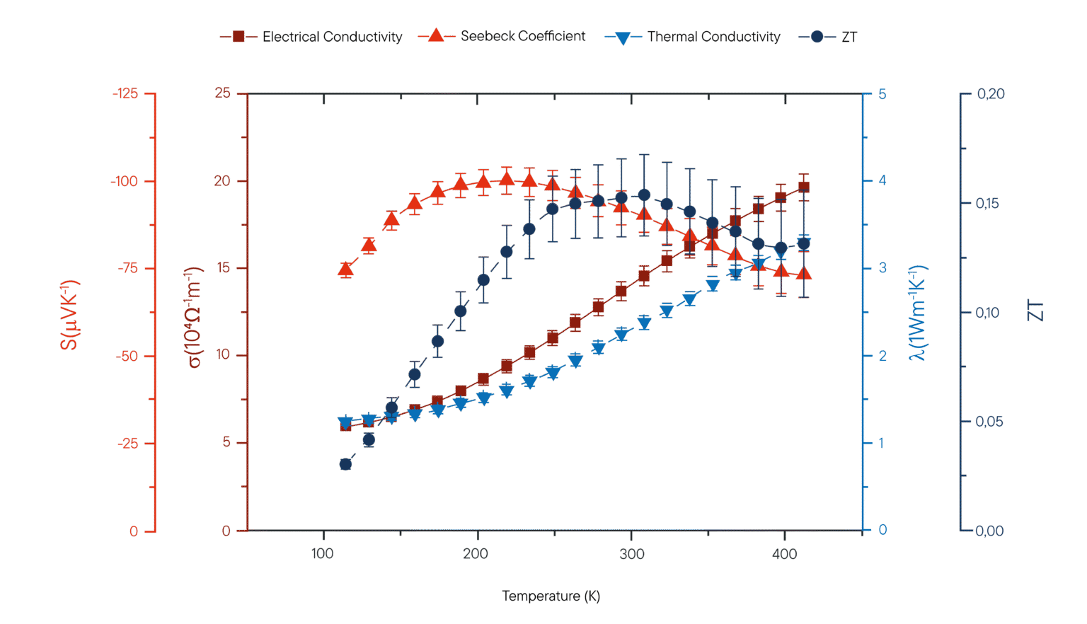
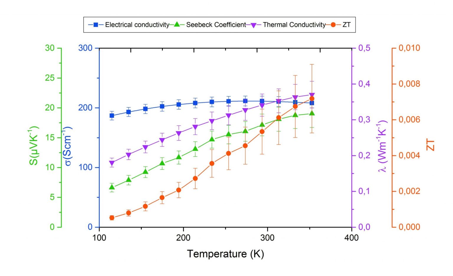
Application Case 2: Thin-Film Electrical Transport Properties and Thermoelectric Effect Measurement (Van der Pauw / Seebeck / Electrical Conductivity)
Thin-film technology is widely used in thermoelectric materials, sensor devices, and optoelectronic applications. In addition to thermal conductivity, electrical transport properties (such as electrical conductivity and Seebeck coefficient) are also critical to performance. Using chip-based measurement platforms, both electrical and thermal measurements can be performed on thin films.
Measurement and analysis focus:
- Four-probe Van der Pauw measurement configuration: High-accuracy determination of thin-film resistivity and carrier concentration.
- Seebeck coefficient measurement: Evaluation of thermovoltage generated under a temperature gradient for thermoelectric device design.
- Thin-film-specific sample support: Suitable for ultrathin (<100 nm) measurements, considering interface effects, grain structure, and process-induced variations.
These measurements are applicable to research on thermoelectric thin films, OLED encapsulation films, MEMS sensing films, and other microelectronic thin-film systems.
Overview of Common Thermal Analysis and Thermophysical Property Measurement Techniques for Thin-Film Technology
- Laser flash analysis (TF LFA): Measurement of thermal diffusivity and thermal conductivity for thin films and multilayer structures.
- TFA (Van der Pauw, Seebeck): Carrier concentration and thermoelectric performance analysis for thermoelectric and sensing thin films.
- Thermomechanical analysis / dilatometry (TMA / DIL): Measurement of expansion, stress relaxation, and dimensional stability of thin film–substrate systems.
- Multilayer sample modeling and thickness-dependent analysis: Systematic evaluation of the impact of film thickness on thermal/electrical performance.
- Specific heat capacity determination (Cp): Providing thermodynamic baseline data for thin-film thermal design and simulation.
Based on thin-film material types (such as phase-change films, thermoelectric films, thermally conductive films, display films, and microelectronic films) and process conditions (CVD, ALD, PVD, printing processes, etc.), we assist in planning the most suitable measurement techniques and experimental workflows, and provide feasibility testing and technical support services to enable R&D, production, and reliability assessment.
Do You Need Thermophysical and Electrical Property Evaluation Solutions for Thin-Film Materials?
We provide measurement services, technical consulting, and project collaboration to help you improve R&D efficiency and thin-film application reliability.
Allen Kuo|FST International|Email: Allen.kuo@fstintl.com.tw